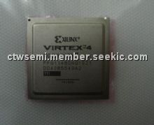
Product Summary
The XC4VLX100-11FFG1148I is a user-programmable gate array with various configurable elements and embedded cores optimized for high-density and high-performance system designs. All IP cores for the XC4VLX100-11FFG1148I are found on the Xilinx IP Center Internet portal presenting the latest intellectual property cores and reference designs via Smart Search for faster access. The wide array of the XC4VLX100-11FFG1148I hard-IP core blocks includes the PowerPC processors (with a new APU interface), tri-mode Ethernet MACs, 622 Mb/s to 6.5 Gb/s serial transceivers, dedicated DSP slices, high-speed clock management circuitry, and source-synchronous interface blocks.
Parametrics
XC4VLX100-11FFG1148I absolute maximum ratings: (1)Internal supply voltage relative to GND:–0.5 to 1.32 V; (2)Auxiliary supply voltage relative to GND:–0.5 to 3.0 V; (3)Output drivers supply voltage relative to GND:–0.5 to 3.75 V; (4)Key memory battery backup supply:–0.5 to 4.05 V; (5)Input reference voltage:–0.3 to 3.75 V; (6)I/O input voltage relative to GND (all user and dedicated I/Os):–0.75 to 4.05 V; (7)I/O input voltage relative to GND (restricted to maximum of 100 user I/Os):–0.95V to 4.4V (Commercial Temperature),–0.85V to 4.3V (Industrial Temperature); (8)2.5V or below I/O input voltage relative to GND (user and dedicated I/Os):–0.75 to VCCO + 0.5V; (9)Current applied to an I/O pin, powered or unpowered:±100 mA; (10)Total current applied to all I/O pins, powered or unpowered: 200 mA.
Features
XC4VLX100-11FFG1148I features: (1)1.5 to 3.3 V I/O Operation; (2)Built-In ChipSync Source-Synchronous Technology; (3)Digitally-controlled impedance (DCI) active termination; (4)Fine grained I/O banking (Configuration in one bank); (5)Flexible Logic Resources; (6)Built-in System Monitor (voltage/temp. measurement); (7)10-bit, 200kSPS A/D Converter (ADC); (8)Secure Chip AES Bitstream Encryption; (9)90-nm copper CMOS process; (10)1.2V core voltage; (11)Flip-Chip Packaging; (12)RocketIO 622 Mb/s to 11.1 Gb/s Multi-Gigabit ; (13)Transceivers (MGT); (14)IBM PowerPC RISC Processor Core; (15)18x18, two’s complement, signed Multiplier; (16)Optional pipeline stages; (17)Built-In Accumulator (48-bits) & Adder/Subtracter.
Diagrams

| Image | Part No | Mfg | Description |  |
Pricing (USD) |
Quantity | ||||||
|---|---|---|---|---|---|---|---|---|---|---|---|---|
 |
 XC4VLX100-11FFG1148I |
 |
 IC FPGA VIRTEX-4LX 100K 1148FBGA |
 Data Sheet |

|
|
||||||
| Image | Part No | Mfg | Description |  |
Pricing (USD) |
Quantity | ||||||
 |
 XC4VFX100-10FF1152I |
 |
 IC FPGA VIRTEX-4FX 1152FFBGA |
 Data Sheet |

|
|
||||||
 |
 XC4VFX100-10FF1517I |
 |
 IC FPGA VIRTEX-4FX 1517FFBGA |
 Data Sheet |

|
|
||||||
 |
 XC4VFX100-10FFG1152C |
 |
 IC FPGA VIRTEX-4FX 100K 1152FBGA |
 Data Sheet |

|
|
||||||
 |
 XC4VFX100-10FFG1152I |
 |
 IC FPGA VIRTEX-4FX 100K 1152FBGA |
 Data Sheet |

|
|
||||||
 |
 XC4VFX100-10FFG1517C |
 |
 IC FPGA VIRTEX-4FX 100K 1517FBGA |
 Data Sheet |

|
|
||||||
 |
 XC4VFX100-10FFG1517I |
 |
 IC FPGA VIRTEX-4FX 100K 1517FBGA |
 Data Sheet |

|
|
||||||
 (China (Mainland))


